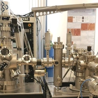
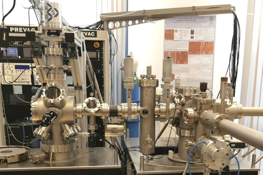
Niskotemperaturowy skaningowy mikroskop tunelowy
Mikroskop wykorzystuje kwantowe zjawisko tunelowania elektronów pomiędzy próbką a ostrzem skanującym. Mikroskop pozwala m.in. na obserwowanie powierzchni próbki z rozdzielczością atomową, obrazowanie struktury cząsteczek, defektów, czy też badanie lokalnej gęstość stanów elektronowych (w opcji zwanej skaningową spektroskopią tunelową, STS). Pomiary można wykonywać w warunkach ultrawysokiej próżni (poniżej 1*10-10 mbar) w szerokim zakresie temperatur od ~10 K do 400 K. System chłodzenia pracuje w obiegu zamkniętym, bez konieczności zakupu ciekłego helu. Jest tak zaprojektowany, aby umożliwiał chłodzenie nie tylko samej próbki, ale i ostrza. Znacznie zwiększa to rozdzielczość i w znacznym stopniu ogranicza wpływ szumu termicznego na mierzony sygnał.
Mikroskop jest zainstalowany w dwukomorowym systemie ultrawysokiej próżni, który umożliwia przygotowywanie próbek (wygrzewanie, bombardowanie jonami, osadzanie adsorbatów) oraz dodatkową charakteryzację powierzchni przez wyznaczanie jej składu chemicznego (spektroskopia elektronów Augera, AES) i stanu uporządkowania krystalograficznego (dyfrakcja nisko-energetycznych elektronów, LEED). Wszystko to pod kontrolą zawartości gazów resztkowych w tym systemie (kwadrupolowy spektrometr mas, RGA).
Aparatura udostępniania na zasadach wynikających z Regulaminu Korzystania z Infrastruktury Badawczej ACMiN. (https://acmin.agh.edu.pl/home/acmin/5_Wspolpraca/Aparatura/Zasady_i_koszty_korzystania_z_infrastruktury_badawczej_ACMiN.pdf)
Obrazowanie 'topografii' powierzchni przewodzących próbek z rozdzielczością atomową.
Wyznaczanie charakterystyk prądowo-napięciowych (I-V, dI/dV)
Zgrubne pozycjonowanie XYZ: 4 mm x 4 mm x 8 mm
Obszar skanowania: (XY): 6.0 μm x 6.0 μm (@ 300K) 1.5 μm x 1.5 μm (@ 10K)
Rozdzielczość skanowania: atomowa
Minimalny dryft termiczny: 0.2 Å/h (XY) oraz (0.2 Å/dobę (Z)
Temperatura próbki: od 10 K (He) do 400 K
Maksymalny rozmiar próbki: 10 mm x 10 mm
Jednostka odpowiedzialna
Grupa / laboratorium / zespół
Zakład Efektów Kwantowych w Nanostrukturach