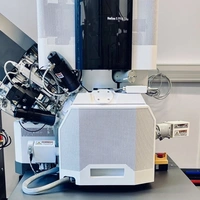
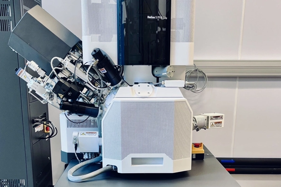
Dwuwiązkowy ultra-wysokorozdzielczy skaningowy mikroskop elektronowy z działem jonów ksenonu (PFIB/SEM) wraz z mikroskopem sił atomowych (AFM)
Dwuwiązkowy, ultra-wysokorozdzielczy skaningowy mikroskop elektronowy Helios 5 wyposażony jest w wysokostabilne, monochromatyczne działo elektronowe z emisją polową Schottky'ego (FEG - Field Emission Gun) oraz działo jonowe Xe (PFIB - Plasma Focused Ion Beam). Umożliwia pracę z napięciem przyspieszającym w zakresie od 350 V do 30 kV (max. prąd wiązki elektronowej 100 nA) i energii lądowania 20 eV do 30 keV. Zdolność rozdzielcza mikroskopu definiowana jako rozdzielczość obrazów elektronów wtórnych przy napięciu przyspieszającym 1 kV na standardowej próbce cząstek złota wynosi 0.7 nm. Maksymalne pole widzenia wynosi 2.3 mm dla WD 4 mm.
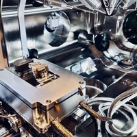
Mikroskop wyposażony jest w:
- detektory do obrazowania: wewnątrzsoczewkowy Elstar (TLD-SE, TLD-BSE); wewnątrzkolumnowy Elstar (ICD - SE/BSE); elektronów wtórnych (ETD); elektronów i jonów wtórnych (ICE - SI, SE); wysuwany niskonapięciowy, wysokokontrastowy detektor elektronów wstecznie rozproszonych (ABS/DBS),
- spektrometr dyspersji energii promieniowania rtg. (EDS - Energy Dispersive X-ray Spectrometer) Ultim MAX 60 oraz kamerę CMOS Symmetry S3 firmy Oxford Instruments umożliwiającą pomiary dyfrakcji elektronów wstecznie rozproszonych (EBSD - Electron Backscatter Diffraction),
- detektor umożliwiający obrazowanie w trybie skaningowo-transmisyjnym (STEM3+),
- działo jonowe Xe (PFIB) i dwa systemy dozowania gazów (GIS - Gas Injection System). Możliwość depozycji platyny (Pt) i/lub wolframu (W),
- nanoindenter FT-NMT04 firmy FemtoTools,
- oprogramowanie Auto Slice&View,
- stolik AFM firmy NenoVision.
Maksymalne wymiary próbek – średnica: 110 mm, wysokość: 65 mm; waga: 500 g.
Aparatura udostępniania na zasadach wynikających z Regulaminu Korzystania z Infrastruktury Badawczej ACMiN. (https://acmin.agh.edu.pl/home/acmin/5_Wspolpraca/Aparatura/Zasady_i_koszty_korzystania_z_infrastruktury_badawczej_ACMiN.pdf)
- Ultra-wysokorozdzielcze obrazowanie mikrostruktury materiałów przewodzących i nieprzewodzących.
- Pomiar nanotwardości.
- Analiza topografii powierzchni (AFM).
- Tomografia elektronowa (SEM/FIB) - rekonstrukcja 3D mikrostruktury.
- Analizy składu pierwiastkowego (EDS).
- Analizy orientacji krystalograficznych (EBSD).
- Przygotowanie próbek TEM i APT bez implantacji Ga+.
- Analiza wielkości i kształtu cząstek i porów, pomiar grubości powłok o rozmiarach mikro- i nanometrycznych.
- Obrazowanie w trybie skaningowo-transmisyjnym (STEM):
- jasnym polu (BF),
- ciemnym polu (DF),
- szerokokątowym ciemnym polu (HAADF).
- Precyzyjne przygotowanie przekrojów PFIB (Rocking Polish).
- Możliwość akwizycji obrazów z dużych obszarów (Mapa 3 SEM).
Jednostka odpowiedzialna
Grupa / laboratorium / zespół
Zakład Materiałów Funkcjonalnych i Nanomagnetyzmu