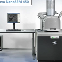
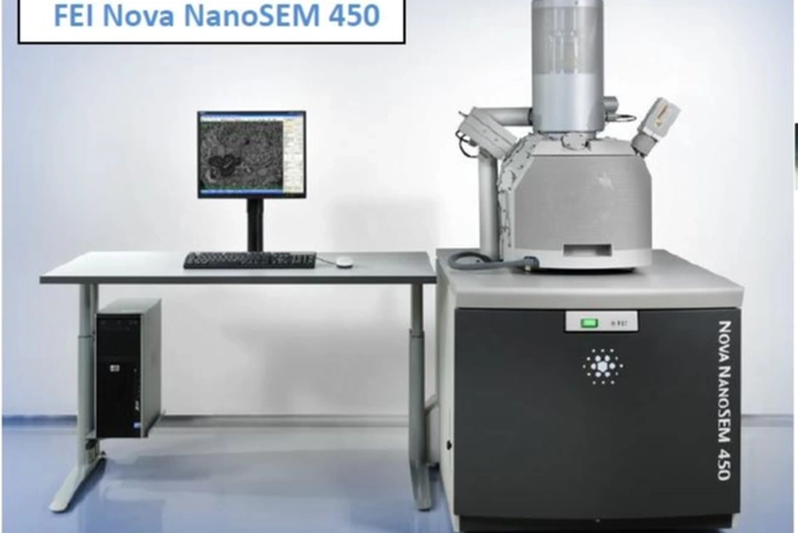
Skaningowy mikroskop elektronowy Nova Nano SEM 450
Źródło elektronów Schottk'ego o wysokiej stabilności prądu wiązki, niska i wysoka próżnia. Detekcja elektronów wtórnych (SE), wstecznie rozproszonych (BSE), TLD-SE i -BSE, tryb transmisyjny (STEM), Możliwości analityczne EDS, EBSD, WDS, Obrazowanie mikrostruktury HR-SEM (SE, BSE) Analiza EDS, WDS składu chemicznego Analizy orientacji krystalograficznych (EBSD) Obrazowanie w trybie STEM
W ramach umów i zleconych zadań badawczych/upoważnienie kierownika Katedry IPiAM
Badania struktury nanomateriałów, morfologii i składu chemicznego próbek nieprzewodzących w niskiej i zmiennej próżni. Analiza topografii orientacji materiałów drobnokrystalicznych z pełną identyfikacją fazową, Analizy punktowe, liniowe oraz powierzchniowe pierwiastków z wykorzystaniem spektrometrów EDXS i WDXS, Analiza orientacji krystalograficznych z wykorzystaniem EBSD oraz transmisyjna dyfrakcja EBSD.
Jednostka odpowiedzialna
Grupa / laboratorium / zespół
Laboratorium skaningowej mikroskopii elektronowej KIPiAM https://kipiam.agh.edu.pl/